05/23 By Dr. Matsakis
Letting The Chips Fall
When my son was all of three years old, he asked me how to make a car. I told him it takes a lot of people to make one, and each person makes one part. He understood that, though it was a little harder explaining carburetors. I never had to tell him about computers. Back then cars didn’t have them. Nowadays, most cars don’t have carburetors but you can find a computer in everything from toasters to Masterclock products.
And how do you fabricate the chips computers use? With a FAB, of course. At one time, every large computer company had a FAB to make its own chips. As AMD’s CEO Jerry Sanders famously said in 1982, “Real men have FABS”. Yet nowadays, few companies own them. That’s because in normal times (i.e. times of peace and harmony), division of labor brings greater efficiency. Separate companies handle the architecture, software, and IP aspects of chipmaking. The actual physical chip can then be made by whoever fabricates them best. That best is usually TSMC, Taiwan Semi-Conductor Manufacturing, which makes 40% of the world’s chip supply [1].
But who makes the machines that make the FABS? Cheap FABS are one thing, but the unquestioned supplier of the very, very best FABS is the ASML corporation [2]. They’ve only made 140 units so far, but if you have $300 million to spare and are a citizen of the free world, you can get in line. One minor problem - you guessed it - the chips shortage is affecting the components ASML needs to make the machines that make the chips.
ASML’s claim to fame is Extreme Ultra-Violet lithography, or EUV, which can make chips with components an order of magnitude smaller [3] than the competing technique DUV [4]. ASML uses laser-made radiation to zap tin beads and create ultraviolet radiation at a wavelength about 13.5 nm [5] , which is guided with extremely flat mirrors to the substrate, which has been coated with photo-resisting chemicals. The required pointing precision is about the size of a coin as seen from the Moon, or the angular size of the first giant black hole (38 billion km, or 1/6 the solar system’s size) imaged by the Event Horizon Telescope, at a distance of 54 million light-years. They can get 10 billion transistors on a chip, with elements going down to 5 nm. Only a few applications need that many, such as Artificial Intelligence and certain warplanes [6]. Microwave ovens can get away with 200-nm size chips, but your car uses chips at the 30 nm, enabling it to do just about everything [7]. The largest FAB-owners are TSMC, Samsung, and INTEL [8]. Interestingly, cooperatively, and doubtless legally, these three customers also own about a fourth of ASML’s stock.
With the U.S. CHIPS act, we can hope that all our chip problems will be solved by 2024 at the latest. Among the FABS being built are three large plants in Texas, by INTEL, TSMC, and Samsung. Their water requirements will be millions of barrels per day, but they can recycle 90% of it.
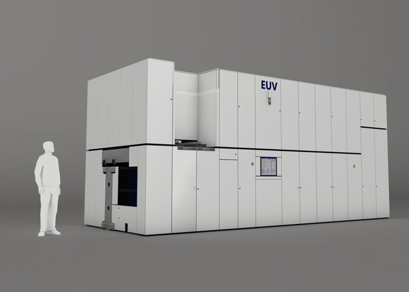 Figure 1. A render depicting the form and scale of ASML's EUV machine.
So if my grandchild ever asks me how a computer is made, I won’t say that it takes many persons. I’ll say that it takes a FAB, and a FAB works because it is relies on the participation of many companies, with each company handling one aspect.
Footnotes
[1] It is unclear whether being the advanced chip-production center makes the People’s Republic of China more likely to invade Taiwan, or whether an invasion is impeded by fears the resource would be destroyed in the fighting.
[2] ASML used to mean Advanced Semi-conductor Materials Lithography. It makes components all over the world, assembles the equipment in the Netherlands, and then dis-assembles the machine for shipment to customers.
[3] When it comes to computers, small is beautiful in every way. They run faster, use less energy, create less heat, and as a result can do more.
[4] DUV=Deep Ultra-violet lithography system. INTEL can make FAB equipment using this.
[5] A nanometer (nm) is a billionth of a meter (m). A silicon atom is 0.2 nm in size. GPS microwave signals have a wavelength of about 0.2 m – a billion times coarser.
[6] War has driven countless innovations, and also killed off some notable innovators. Peace has done the same.
[7] The distinction between auto mechanics and computer technicians is certainly fading. Have you noticed that “real men”, and even “real women”, don’t do their own auto repairs anymore? I changed a wiper-blade last year.
[8] In a surprising lack of foresight for a company founded by Moore himself, INTEL lost a big chance to upgrade its facilities 20 years ago, when they turned down a request from Apple to go with smaller size chip elements for its iPhone. But they haven’t given up and are developing a technique they call High-Numerical-Aperture, that will hopefully create even smaller size elements. The internet tells me that “Plaid UV”, or PUV also be a technique to watch. This one uses fusion-like techniques instead of blasting tin beads.
About Dr. Demetrios Matsakis
 Dr. Demetrios Matsakis attended MIT as an undergraduate and received his PhD in physics from UC Berkeley, where he studied under the inventor of the maser and laser; and built specialized ones in order to observe interstellar dust clouds where stars are born. His first job was at the U.S. Naval Observatory, building water vapor radiometers and doing interferometry to observe quasars and galaxies at the edge of the observable universe. After developing an interest in clocks, Dr. Matsakis would spend the next 25 years working hands on with most aspects of timekeeping – from clock construction, to running the USNO’s Time Service Department, to international policy. He has published over 150 papers and counting, but gets equal enjoyment out of beta-testing his personal ensemble of Masterclock products.
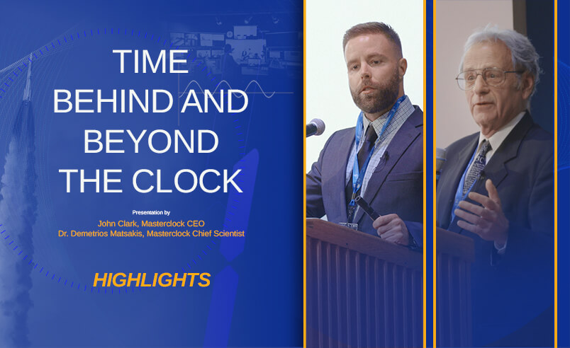
Presentation by John Clark, CEO & Dr. Demetrios Matsakis, Chief ScientistTime Behind and Beyond the Clock